Electron and scanning probe microscopy
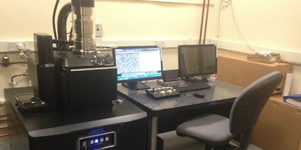
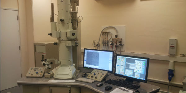
The Electron and Scanning Probe Microscopy Unit provides solutions for imaging and analysis at the nanoscale. The unit houses two scanning electron microscopes, two scanning probe microscopes and three transmission electron microscopes.
The electron microscopes in the main suite are all fitted with digital image capture and energy dispersive X-ray systems for analysis of elemental composition and distribution. The most recent additions are a Jeol 1400 TEM and Jeol IT300 SEM. A Gatan Cathodoluminescence detector has also been installed on our existing Field Emission Gun SEM. In 2015 a new high resolution analytical FEG-TEM will be installed.
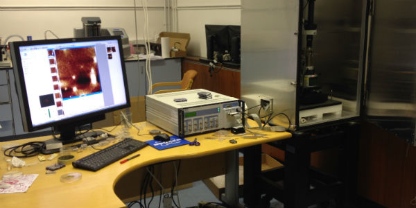
Both modular SPM microscopes are capable of atomic resolution imaging as well as numerous other imaging and analytical modes. One Bruker Multimode system has recently been upgraded with Peakforce technology to allow conductivity and quantitative material property (including modulus, adhesion, deformation, and dissipation) mapping.