Advanced gate driving
The power electronics industry is poised to undergo significant change, as ultra-fast-transition transistors made from silicon carbide (SiC) and gallium nitride (GaN) have recently emerged. These could push efficiencies to levels never achieved before, but only if extremely short switching transitions (below 10 nanoseconds) can be achieved. Fast switching is challenging, however. For example, it produces high electromagnetic emissions. Over the past years, the Electrical Energy Management Group has developed a range of novel gate-driving techniques, to help industry adopt SiC and GaN, and increase the power throughput of power converters whilst reducing electromagnetic emissions.
What is active gate driving?
Gate drivers normally apply a constant voltage to a gate (e.g. 5 V) to turn on a power semiconductor device. Applying 0 V turns it off. Instead of this single step, an active gate driver shapes the gate voltage in order to improve switching waveforms. Active gate driving for silicon power electronics is generally carried out using analogue closed-loop techniques, where the drain-source voltage is made to follow a desired reference voltage.
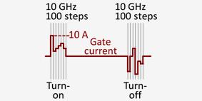
For GaN, faster techniques are required. We use an 800 MHz clock to trigger much faster asynchronous pulse trains, which complete in a single clock cycle. In this way, the gate signal can be changed once every 100 ps, which equates to an update rate of 10 GHz.
During most of the switching process, the driver operates as a current source, as the output transistors are saturated. As the gate voltage approaches the driver's maximum output voltage, the driver resembles a voltage source with a programmable output resistance.
For more information on our Advance Gate Driving research please visit:
For more information on our Advance Gate Driving research please visit:
- GaN and its challengesGaN power transistors (labelled “GaN” in figure) are the latest and fastest power devices to emerge on the market. We have developed an integrated, 10 GHz active gate driver for GaN FETs.
- Elimination of voltage overshootThe active gate driver almost entirely eliminates voltage overshoot in hard-switched circuits
- Reduction of EMI from a GaN bridgeEMI in the band from 300 MHz upwards is reduced without increasing switching loss.
- Active gate driving of IGBTsSilicon power electronic devices such as IGBTs and MOSFETs can be controlled via the gate. Active gate driving produces switching waveforms with less electromagnetic interference.
- Resonant gate drivers for SiC MOSFETsThese silicon gate drivers can be located at a safe distance from wide-bandgap power devices with a higher thermal rating, and the energy used to charge the gate can be recycled.
- Other gate driversWe are keen to experiment with new driver architectures, to develop drivers that fully exploit emerging power devices, or to develop drivers for applications where existing drivers pose unwanted limitations.