Low Dimensional Materials & Devices
Many bulk materials can be thought of as nearly two-dimensional (2D) or one-dimensional (1D). This is because of the symmetry and chemical make-up of their crystal structures.
The images below show schematics of the electronic structure and the crystal structure of LaFePO and Li0.9Mo6O17. These materials behave electronically in a quasi-1D and quasi-2D manner, respectively.
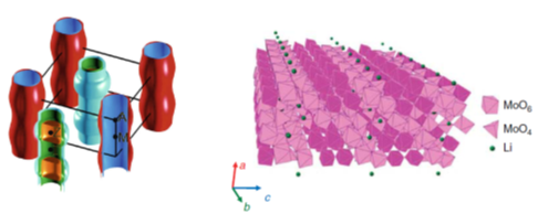
Left: The calculated Fermi surface of the pnictide superconductor LaFePO (without spin–orbit corrections) from Carrington et al 2009. Right: Crystal structure of the 1D conductor Li0.9Mo6O17 from Wakeham et al 2011.
Lower dimensions are interesting since the correlated physics changes. For example, the nature of superconductivity in reduced dimensions is quite different from the three-dimensional system. This broad area in 2D was the topic of the Nobel Prize in Physics in 2016. In 1D further exotic physics can occur such as spin-charge separation in Tomonaga–Luttinger liquids.
Materials can also be made 2D by growing them as thin films. The dimensionality is then a tuning parameter, together with new controls such as the substrate the thin film is grown on. The crystal thin film can follow the substrate atomic arrangements in some way (epitaxy), which can generate large compressive or tensile strains in the crystal. This changes the equilibrium thermodynamic state of the system.
We can also make heterostructures of different materials. Here, entirely new physics can emerge at the interfacial regions.
An interesting question is how thin do you need to be to show 2D physics? The answer depends on the type of physics you are looking at. For example, in superconducting semiconducting thin layers the superconductivity is 2D before the electronic structure shows signs of 2D character (see figure below).

Left: Schematic of a 'delta'-doped superconducting semiconductor thin film of SrTiO3, where the electron donor Nb is added only in a thin layer. Right: A resultant phase diagram showing transitions from 3D to 2D for the superconducting (transition temperature, blue) and normal state (electron mobility, red) from Kim et al 2011.
Once we have a thin film, we can also make device structures such as transistors (below). Here, the physical properties are controlled by a gate voltage.
The gate voltage can control the carrier density; electron mobility; the strength of the spin-orbit coupling; or even the long range ordered states such as superconductivity or magnetism. This opens up the possibility of exploring fundamental physics, such as the quantum critical behaviour of systems when their ordering temperatures are tuned close to absolute zero. This also points to possible applications such as magnetic memory devices with voltage tuneable properties.
