Diagnosing contact failure in computer chips
When computer chip prototypes fail, our focused ion beams provide a manufacturing solution.
Challenge
Before being manufactured in the millions, silicon computer chips have to be prototyped and tested to ensure that the design is perfectly functional.
The metal wires and integrated circuit connections are arranged in delicate micrometre layers, and can only be viewed with high resolution electron microscopes.
When engineers discover a prototype is malfunctioning, the sample needs to be inspected and sectioned by a focused ion beam, before the integrated circuit can be inspected with an electron microscope.
Solution
Using a focused ion beam (FIB) the semiconductor chip was sectioned into very thin slices, allowing the integrated metallic layer beneath the surface circuit contact point to be removed and investigated using an SEM and TEM.
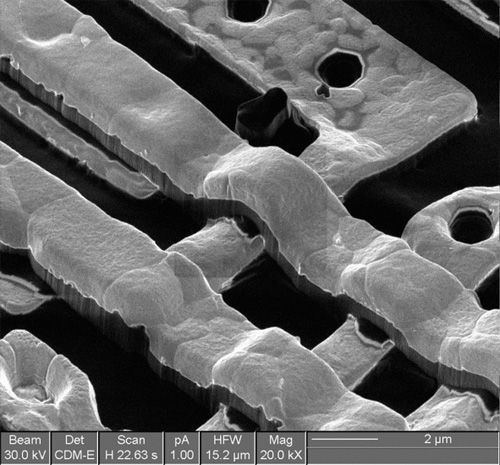
A closer look at where the circuit’s contact has failed, using SEM
Courtesy of Peter Heard
On the Dual Beam instrument, the element distribution can also be mapped using EDX analysis, and any faults diagnosed.
Using the FIB and micro-scale platinum deposits, any contact faults were accurately repaired.
Impact
The repair and nature of contact failures that are difficult to diagnose in simulations or by testing the chip is crucial to be done quickly, so that the company can manufacture the chips as soon as possible.
Bristol has offered a turn-around of roughly a week for these kind of repairs and fault analyses, saving a lot of money and quickly pinpointing the nature of the failure.