High resolution imaging and chemical analysis combined
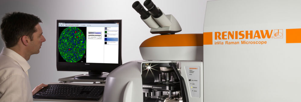
Combining electronic imaging technology with optical chemical analysis has created a system that can image samples with a resolution of 1nm and perform chemical analysis using Raman spectroscopy.
When researchers need high-resolution images of a sample, they often use a scanning electron microscopy (SEM) to get images with a resolution down to one nanometer (1nm).
This powerful tool can also be adapted to perform basic elemental analysis using x-rays. But if researchers need to identify compounds in the sample, they need to use a second technique such as Raman spectroscopy. This involves moving the sample between two instruments and risking analysing the wrong sample region or degrading the sample.
When UK engineering company Renishaw wanted to develop a system that could both image and analyse, the company turned to Dr John Day at the University of Bristol’s Interface Analysis Centre for help.
“I was commissioned to design and develop a novel fibre optic coupled system to acquire co-localised Raman spectra from within an SEM, at the centre of the SEM image” says Day. “This had never been done before.”
The research brief was for an instrument to obtain spectra, with high spatial resolution, from the same sample position viewed by the SEM without impeding any other analytical functions.
This was a challenge because Raman spectroscopy relies on optical phenomena whereas the SEM uses electrons. Also Renishaw insisted that the Raman spectra were obtained from exactly the same spot from which the SEM image was obtained – a spot with a diameter of just one micron (one micrometer, 1μm).
“As well as the challenges of combining an optical technique with an electronic one, we also had to ensure that the optical probe was retractable – researchers did not want the optical probe in the sample area all the time as it can get in the way,” said Day. “This was a challenge because SEM imaging is performed under vacuum.”
Day and his colleagues worked together to design a novel kinematic mount and a double parabolic, aberration correcting focussing system. They also had to design an optical system with a hole in it to allow electron beam to pass through. The resultant fibre optic coupled system was capable of obtaining spectra from a 1μm spot with an efficiency equal to conventional laboratory Raman systems.
The technology developed during this collaboration was patented by Renishaw and today the company remains the only manufacturer of a combined SEM Raman system that images and analyses from the same spot on the sample - selling several systems per year, mainly for export.
The system allows researchers to image the sample and positively identify chemical compounds or distinguish between allotropes such as graphite and diamond. It is used in many applications including the identification of contaminants in semiconductor fabrication lines and the investigation of oxidation in reactor steel.
The development of this system has enabled Renishaw to obtain new customers and secure jobs at its sites in the UK. Ken Williams, international sales manager at Renishaw said: “Dr Day has made a significant contribution to the project that has enabled us to produce a novel combined technology. The interface remains a unique offering that is a high value capital item. We have made and continue to make regular sales of these systems, the majority of which have gone for export. This product has assisted the Spectroscopy Division of Renishaw PLC commercially and in maintaining Renishaw’s position as a world leading supplier of Raman spectrometers.”
Related research groups
Funders
 Study Physics
Contribute to cutting edge research at the very frontier of scientific knowledge.